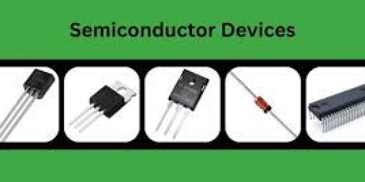
As physical physics limitations make it increasingly difficult and prohibitively expensive to shrink traditional monolithic transistors any further, the electronics industry is embracing a revolutionary design methodology focused on advanced component packaging. Within the competitive matrix of the Semiconductor Device Market growth landscape, the implementation of heterogeneous chiplet architectures has emerged as the primary mechanism to extend performance scaling beyond traditional boundaries. Instead of forcing an entire system onto a single massive piece of silicon, engineers are breaking designs down into smaller, functional modular components called chiplets, which can be manufactured using different optimized transistor nodes and then linked together on a high-speed silicon substrate. This modular assembly approach dramatically improves manufacturing yield rates, lowers overall research and development costs, and allows designers to combine diverse functional elements like memory, analog routing, and digital logic into a single highly integrated package.
However, binding separate chiplets into a singular cohesive processing unit introduces complex engineering hurdles regarding inter-chip communication bandwidth and structural thermal dissipation. Advanced structural packaging techniques, such as three-dimensional vertical die stacking and high-density organic substrates, require microscopic interconnects called through-silicon vias to route electrical signals between layers with minimal latency. These dense multi-layered assemblies trap localized heat, necessitating the development of advanced thermal interface materials and microfluidic cooling channels embedded directly within the component structure. Furthermore, testing these complex multi-die packages requires sophisticated automated diagnostic systems to verify every individual chiplet functions perfectly before final sealing. As consumer electronics demand ever-smaller form factors and high-performance computing centers require unmatched processing density, the mastery of advanced packaging will serve as a vital differentiator for leading global component suppliers.
What exactly is a chiplet architecture, and how does it improve semiconductor manufacturing efficiency? A chiplet architecture breaks a large processor down into smaller functional modules that are manufactured separately and connected together, which improves manufacturing efficiency because smaller dies are less prone to defects, maximizing production yields.
What are through-silicon vias, and why are they necessary in three-dimensional die stacking? Through-silicon vias are vertical electrical connections that pass completely through a silicon die, allowing multiple stacked chips to communicate directly with each other with the shortest possible path, minimizing data latency and power use.
➤➤➤Explore MRFR’s Related Ongoing Coverage In Semiconductor Industry:
Touch Display For Household Appliances Market
Volatile Organic Compound Gas Sensor Market
Wearable Robotic Exoskeleton Market
Advanced Oxidation Process Aop Water Treatment Services Market